T41-EP [Part 1] Software Defined Transceiver
Intro#
A few months back I was working on the KeithSDR transceiver. I got to that project a little bit late and there was not much activity going on at that time. In addition, the transceiver does not include its own RF stage and instead relies on a HobbyPCB SDR, which is no longer available.
As a result, I ended up building my unit as a receiver-only device, limited to the 20-meter band, using a QRP Labs receiver module. Although any IQ RF receiver could potentially work with this project, the T41-EP began to draw my attention, and I eventually considered my KeithSDR project complete.
In this post, I introduce the T41-EP project and describe the journey of building and testing the main PCB.
T41 EP#
The T41-EP project is an open source, standalone, multi-band (160-6 m), HF amateur radio transceiver supporting SSB and CW modes. It is based on the Teensy 4.1 processor. Most of the project information—such as BOMs, schematics, manuals, and PCB Gerber files—can be found in the GitHub repositories at https://github.com/DRWJSCHMIDT/T41/ and https://github.com/DRWJSCHMIDT/K9HZ, as well as in the SoftwareControlledHamRadio groups.io forum, where there is a very active discussion on wide range of T41 related topics.
There is also a companion T41 book that covers general DSP theory along with specific build and design details for the T41 project addressing both software and hardware aspects of the T41. The software is currently available at https://github.com/KI3P/Phoenix/.
The T41-EP project is intended as an experimenter’s platform. It is modular, with plans for several add-ons and multiple build paths. For example, you can choose a 20 W power amplifier, with plans underway for a 100 W amplifier module. Support for dual receivers is already available, and there are plans for an ATU and a VHF/UHF module. You can also choose from different display sizes: 5, 7 or 9 inches.
Specs
- Multiband: 160-6M
- Transmit power: 20W
- Display: 7" (800x480)
- Power Requirements: 12 to 13.8V DC
- 600 Mhz ARM Cortex M7 processor (Teensy 4.1)
- Real‑time waterfall and spectrum displays (up to 192 kHz)
- Modes: SSB and CW (software defined)
- I²C Control: Many modules (front panel, encoders, switch matrix, filters) communicate over I²C
Preparation#
Sourcing the PCBs
I spent several hours reading the forum to gain a better understanding of the project, and when the time came, I joined a PCB group buy to obtain all the boards I needed at an affordable price. At that point, v12.6 was the most recent version, so I purchased a full set of PCBs to build the v12.6 version of the transceiver.
| PCB |
|---|
| v12 main board |
| v12 RF board |
| K9HZ Front Panel |
| K9HZ Encoder (x4) |
| v12 BPF board |
| K9HZ LPF Set |
| 20W PA |
| XMIT Filter Board |
| XMIT Filter Daughterboard |
At the time of doing the group buy, the 100 W PA was not available and I now regret not purchasing the required boards for a second receiver.
Sourcing the components
The next step was to obtain all the components needed to build the T41. I followed the BOMs available in the T41 and K9HZ GitHub repositories. This required placing orders with Mouser, DigiKey, Tayda Electronics, Kits And Parts (for the toroids) and PRJC for the Teensy 4.1 and Audio Hat, as well as ordering the 7-inch display from BuyDispay.com
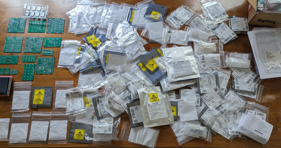
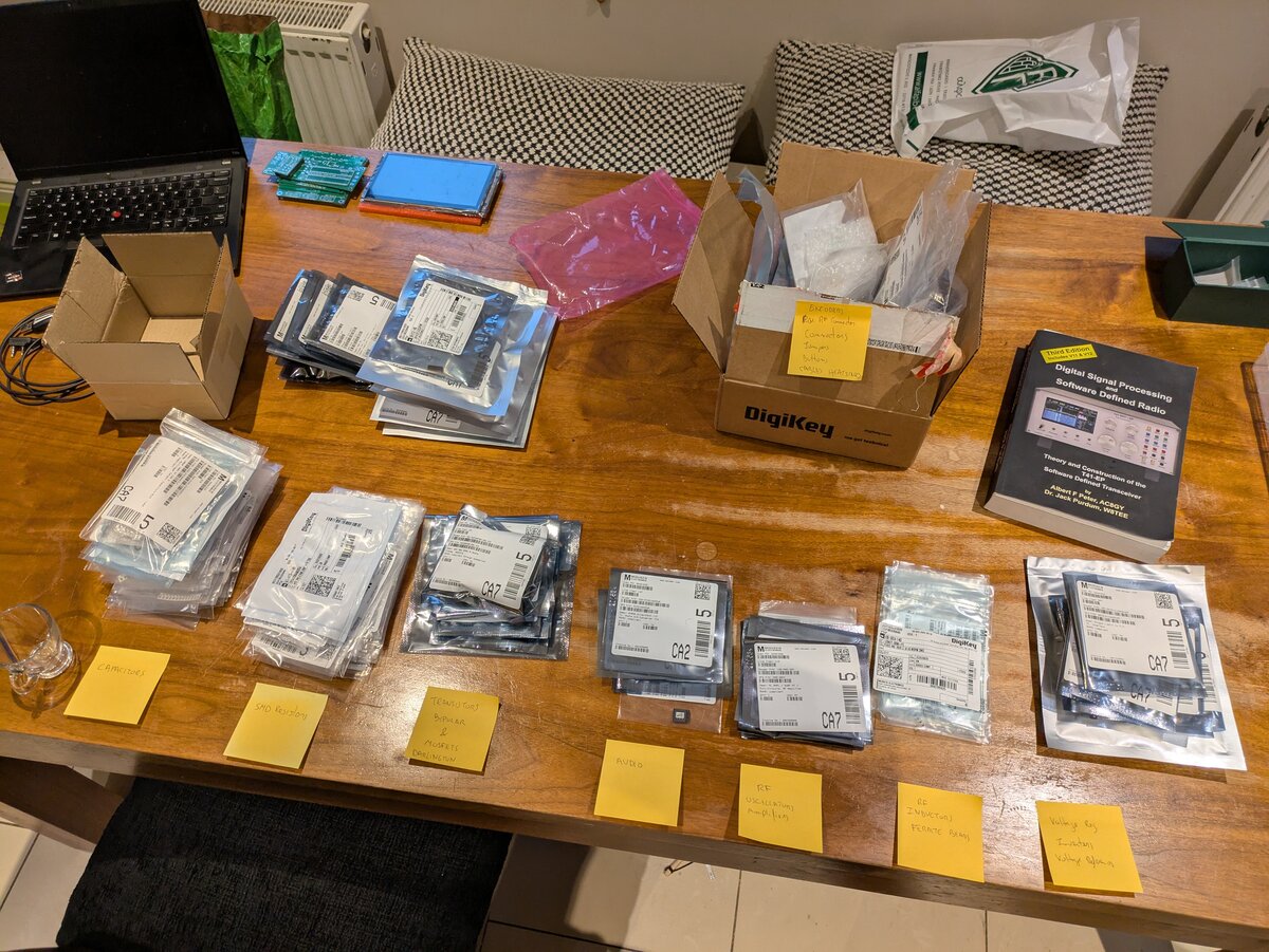
Classifying the parts
Since I ordered components for all PCBs at once—and there were many small ziplock bags containing very small SMD components—I decided to organize everything before starting assembly. I grouped the ziplock bags by component type (resistors, capacitors, inductors, voltage regulators, etc.) and used elastic bands to keep each group together.
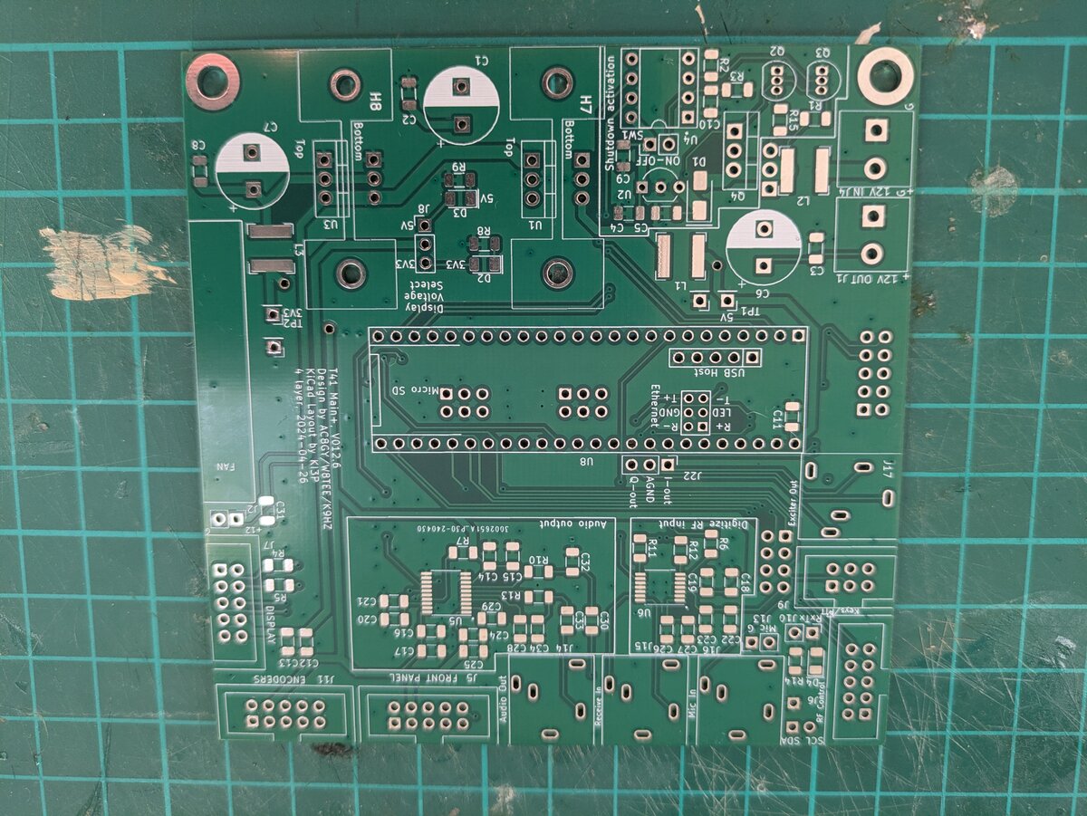
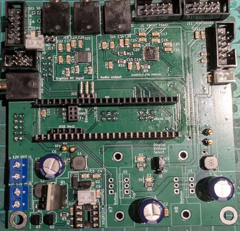
Main Board#
The starting point is the main board. To prepare for assembling the main PCB, I first printed the BOM, the schematic and the assembly manual. I then selected the required components from the organized collection and placed all the components needed for the main board—still inside their plastic bags—into a box.
The plan was to solder each component and discard the bag if it was empty, or return it to the organized stock if any components were left over (some parts are used on multiple boards). However, most of the components were unique to this board, so once the assembly was complete, there would be a significantly less clutter to deal with.
The main board contains several functional sections: a power supply providing 12 V, 5 V and 3.3 V and re-distributing 12 V to the remaining boards; the DAC and ADC converters; a soft On/Off power circuit based on an ATtiny85 microcontroller; the Teensy 4.1 as the main CPU; and the Teensy Audio Hat as the audio interface. The board also includes the connectors for the display, all I²C devices, audio connectors for the IQ audio signals to and from the RF board, and audio input/output for the microphone and speakers.
Power shutdown options
The main board supports two different shutdown methods:
- A basic reverse polarity protection scheme, also used in the v11 boards.
- A smart On/Off switch based on the ATtiny85 microcontroller. When the power-off button is pressed, the ATtiny85 signals the Teensy 4.1, allowing it to run a shutdown routine. Once a gracefull shutdown is complete, the Teensy signals back to the ATtiny85, which then completes the power-off sequence and turns the radio off.
I opted to build option 2.
I started by soldering the ADC and DAC ICs, followed by all SMD components (resistors, capacitors, inductors and the 3 LEDs). The ADC and DAC are by far the most challenging components to solder due to their small size. I used a hot-air gun to solder them in place.
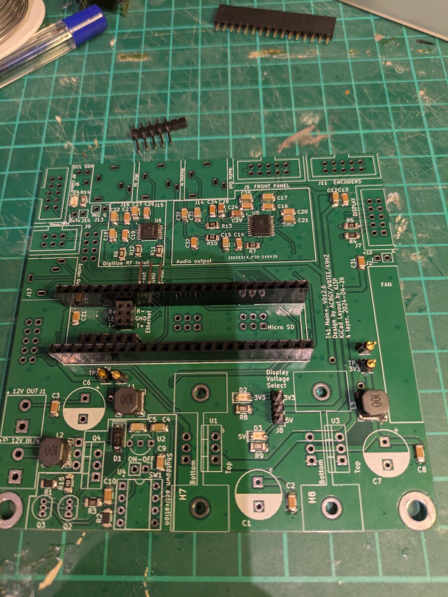
Finally, I added all IDC sockets, power connectors, electrolytic capacitors and the remaining through-hole components. The assembly manual specifies the recommended order for installing these parts.
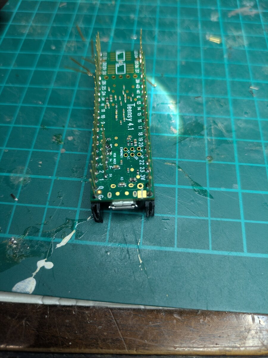
Teensy 4.1 preparation
The Teensy 4.1 requires a set of stacking pin headers so it can be mounted on the main board while allowing the Audio Hat to be plugged on top. When I ordered the parts, I mistakenly purchased a Teensy with standard pin headers already soldered in place for convenience. Unfortunately, I did not anticipate the need for stacking headers to support an additional board on top.
As a result, I had to desolder and clean all the existing pins before soldering the stacking headers—a rather painful process.
The last time I checked the BOM, the stacking pin header was included but with an incorrect quantity specified. This forced me to place an additional order for 1×40 stacking pin headers, which I then cut to the required lengths.
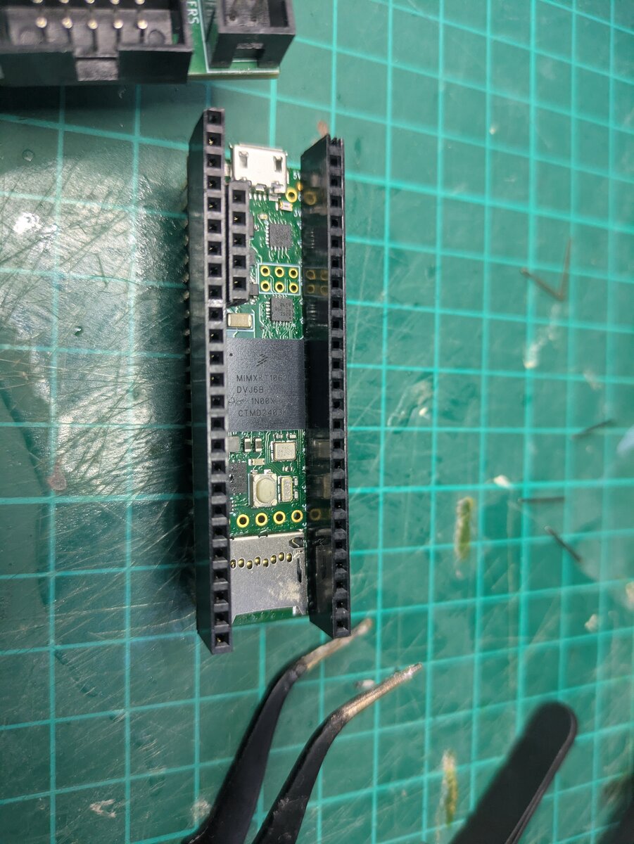
Finally, I had to cut the USB power trace on the Teensy. This prevents the Teensy from being powered up via USB, while still allowing USB connection. The Teensy is instead powered directly by the main boards’s power supply.
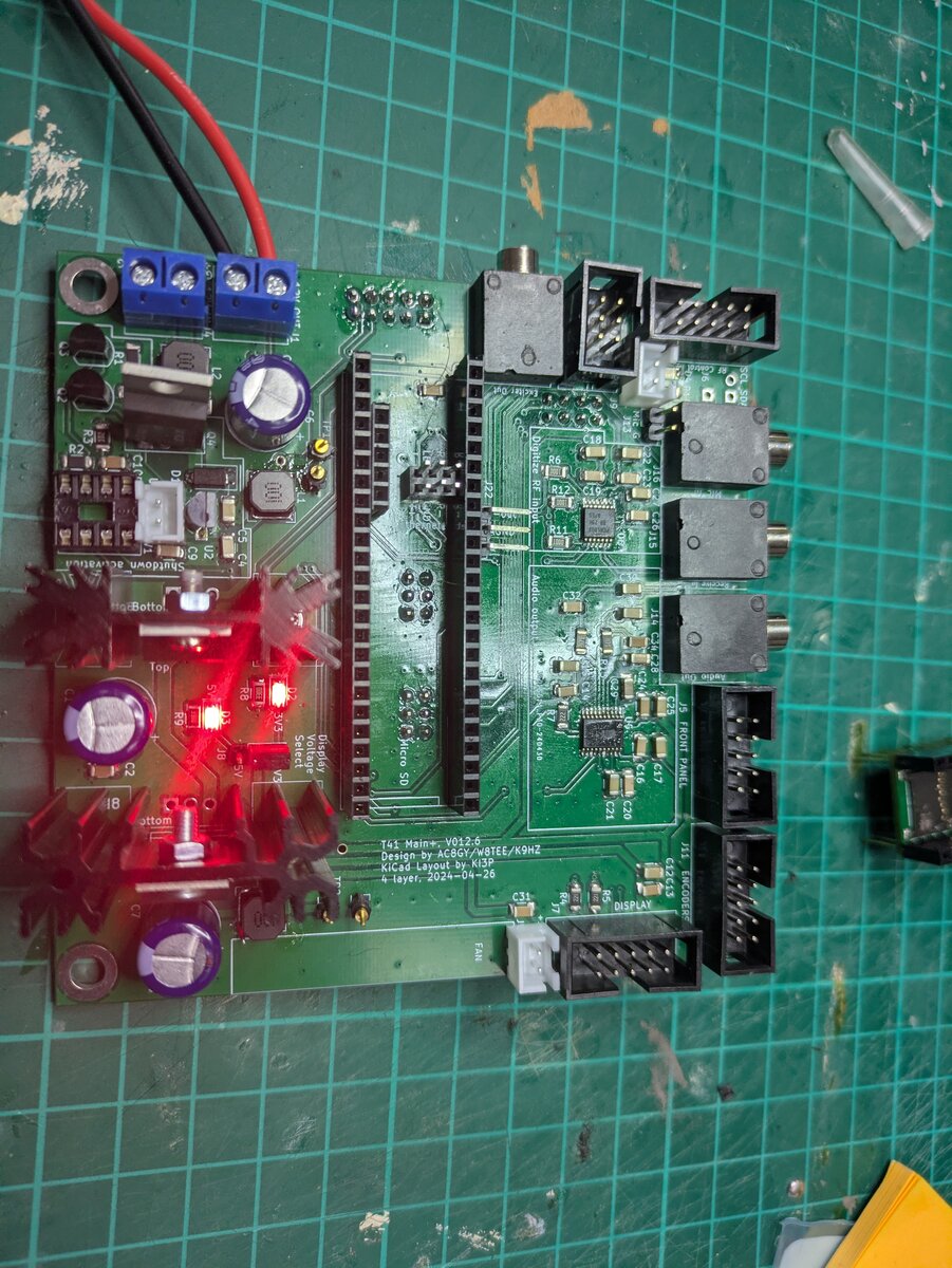
Main board power test
I performed the initial power test by connecting a 12 V power supply to the output power connector, which is used to re-distribute 12 V to the other boards. The reason for connecting the power supply here rather than to 12 V input connector was to bypass the ATtiny85 On/Off switch control circuitry.
As recommended, I performed the first power test with the ATtiny85 removed, the Teensy disconnected, and no other boards attached. If everything is working correctly, the two LEDs corresponding to the 3.3 V and 5 V rails should illuminate. A multimeter can then be used to verify that the correct voltages are present in the test points.
ATtiny85 Programming#
Some kits come with the ATtiny85 pre-programmed, but that was not my case, as I sourced the parts myself. I do not own an ISP (In-serial circuit programmer) for the ATtiny85, but I discovered that an Arduino can be used as an ISP programmer for ATtiny and ATmega devices.
The process consist of the following steps:
- Convert the Arduino into a ISP programmer.
- Wire the ATtiny85 to the Arduino.
- Burn the bootloader onto the ATtiny85.
- Upload the On/Off Switch code to the ATtiny85 using the Arduino as an ISP programmer.
Convert the Arduino into an ISP programmer
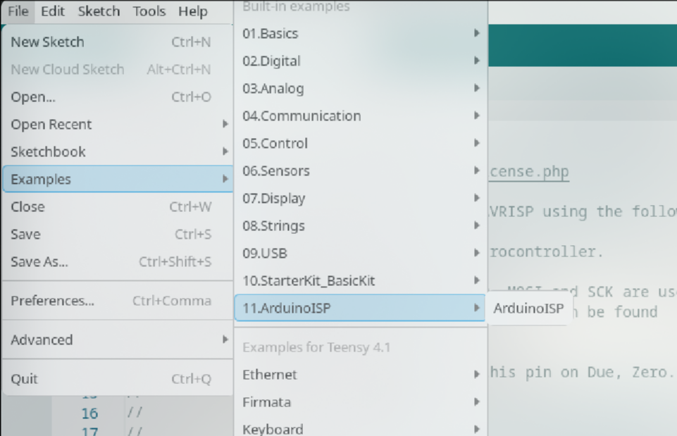
To make the Arduino function as an ISP programmer, I loaded the ArduinoISP sketch from the Examples section of the Arduino IDE onto the Arduino board.
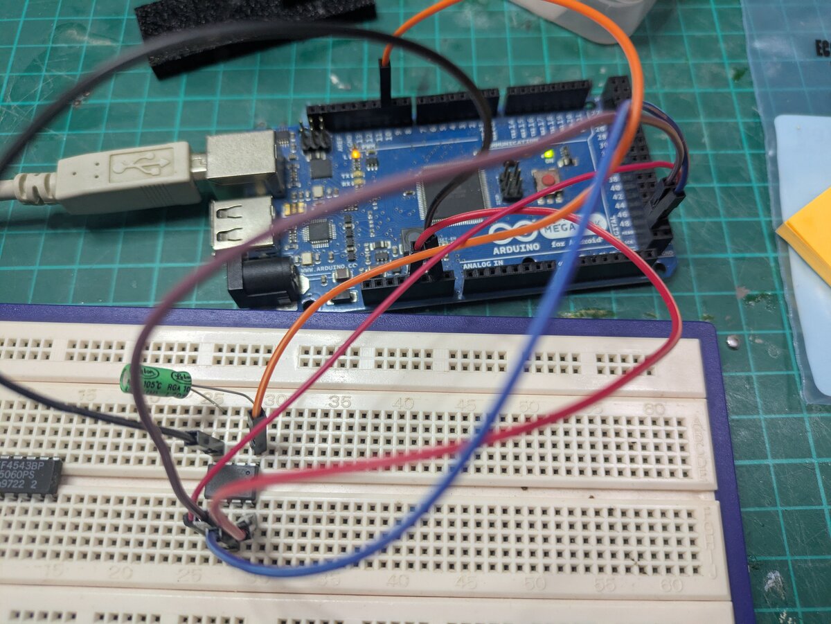
Next, I wired the Arduino to the ATtiny85. The exact connections depend on the Arduino model; I was using an Arduino Mega.
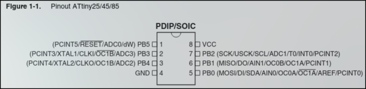
The wiring between the Arduino Mega and the ATtiny85 is as follows (note: it may differ for other Arduino versions):
| Arduino Mega | ATtiny85 |
|---|---|
| 5V | 8 (VCC) |
| GND | 4 (GND) |
| SCK | 7 (SCK) |
| MISO | 6 (MISO) |
| MOSI | 5 (MOSI) |
| 10 | 1 (RST) |
Additionally, I added a 10 µF electrolytic capacitor between RESET and GND, as recommended in the Arduino documentation.
Burn the bootloader
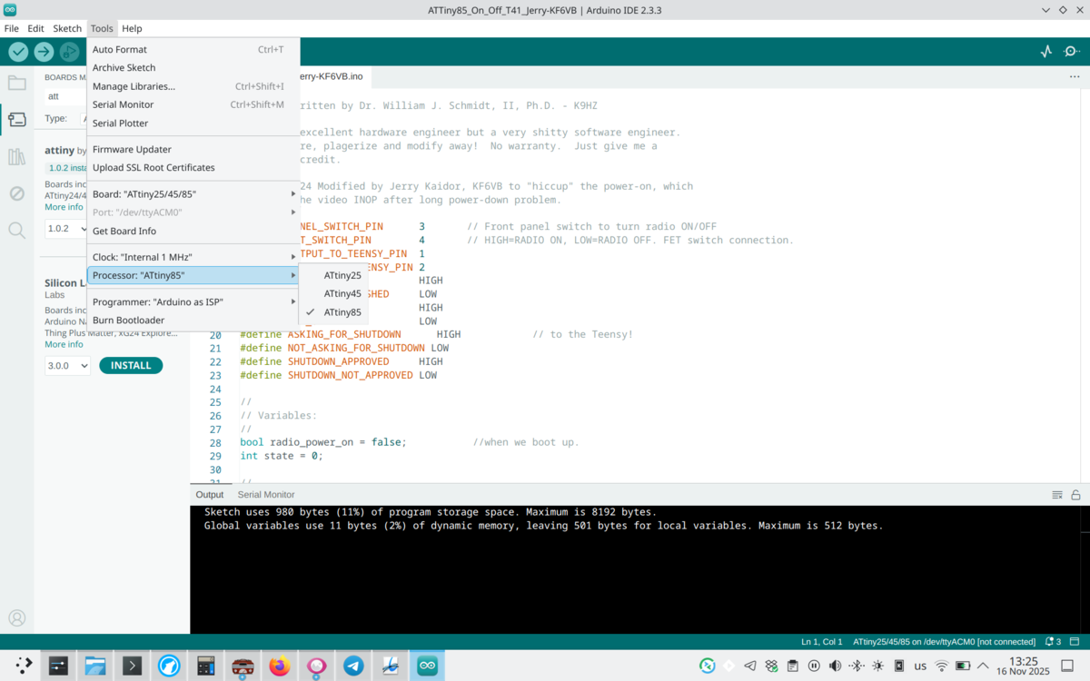
To burn the bootloader onto the ATtiny85, I first needed to install support for ATtiny85 boards in the Arduino IDE:
-
Go to File -> Preferences and add the following URL in the Additional Board Manager URLs field:
https://raw.githubusercontent.com/damellis/attiny/ide-1.6.x-boards-manager/package_damellis_attiny_index.json -
Open Tools -> Board -> Boards Manager, search for “attiny” and install it.
-
Select the right board: Tools -> Board -> ATtiny25/25/85.
-
Select the programmer: Tools -> Programmer -> Arduino as ISP.
-
Select the right processor: Tools -> Processor -> ATtiny85.
-
Burn the bootloader: Tools -> Burn Bootloader
Upload the On/Off smart switch sketch
The ATTiny85_On_Off.ino sketch for the ATtiny85 can be found in the Phoenix repository. I created a directory with the .ino file, opened it in the Arduino IDE, and uploaded the to ATtiny85 using the same options selected in the previous step.
Testing#
For the final tests, I mounted the Teensy and the Audio Hat on top of it. I installed the programmed ATtiny85 and connected the power supply—this time to the input connector. I also connected the Teensy to the computer using a micro-USB cable.
Next, I obtained the Arduino sketches required for testing. I started with the BoarTest/i2cscan sketch. This simple I²C scanner was loaded onto the Teensy, and with the main board powered, I was able to inspect the Arduino IDE serial monitor to see if any I²C devices were detected. At that point the only I²C device connected was the Audio Hat.
Note: To program the Teensy, remember to switch the board type in the Arduino IDE from ATtiny85 to Teensy 4.1. If this is the first time programming a Teensy, installing Arduino IDE Teensy support is required, by following the instructions on the PRJC website. This involves adding the appropriate Additional Board Manager URL in File → Preferences and installing the board package.
Since the power button was still not connected to the board, I shorted SW1 to simulate a button press. This triggered the Teensy startup process.
Upload the i2cscan sketch
After uploading the sketch, the Serial Monitor displayed the following output:
I2C Scanner
Scanning Wire ...
I2C device found at address 0x0A: Teensy audio adapter / hat  !
done

Scanning Wire1 ...
No I2C devices found

Scanning Wire2 ...
No I2C devices found
This confirmed that the Audio Hat was correctly detected on the I²C bus.
At this stage, testing was complete. Next, I will test the 7" display, assemble the Front Panel, Switch Matrix, and Encoder boards, and load the full T41 software.